Ultra-high Resolution SEM Microscope Apreo 2 with EDS/WDS
Scanning Electron Microscopy (SEM) is a powerful imaging technique used to examine the surface structure and composition of materials at high magnifications. It works by directing a focused beam of electrons onto the specimen. As the electrons interact with the surface, they produce various signals (secondary electrons, backscattered electrons, or X-rays) that are detected to form detailed images or provide compositional information. SEM offers high resolution, depth of field, and the ability to analyze micro- to nanoscale features, making it widely used in materials science, biology, and nanotechnology.
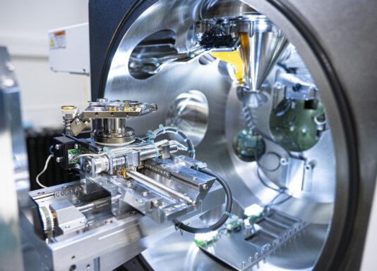
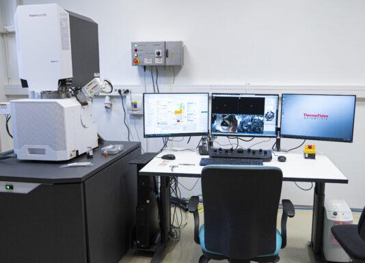
Apreo 2 offers high-quality, high-resolution imaging regardless of the target samples‘ characteristics. In addition to standard, electrically conductive materials, insulators, beam-sensitive materials, magnetic materials, and biomaterials can be investigated. Apreo 2 has Energy dispersive X-ray spectroscopy (EDS) and Wave dispersive X-ray spectroscopy WDS spectrometers for qualitative and quantitative analysis of the chemical composition of samples. An ion gun can clean the samples in situ before observation.
Specification
Resolution
0.9 nm at 1 kV
0.8 nm at 1 kV (beam decel.)
1.0 nm at 1 kV, 10 mm working distance (beam decel.)
0.8 nm at 500 V (beam decel.)
1.2 nm at 200 V (beam decel.)
Standard detectors
ETD, T1, T2, T3, IR-CCD, Nav-Cam+
PivotBeam
Mode for selected area electron channeling (also known as "rocking beam" mode).
Optional detectors
Energy-dispersive X-ray spectroscopy (EDS), wave-dispersive X-ray spectroscopy (WDS)
Landing energy range
20 eV – 30 keV
Stage bias (beam deceleration)
-4000 V to +600 V
Low vacuum mode
10 – 500 Pa chamber pressure
Stage
5-axis motorized eucentric stage, 110 x 110 mm2 with a 105° tilt range. Maximum sample weight: 5 kg in un-tilted position.
Maximum beam current
50 nA (400 nA configuration also available)
Standard sample holder
Multi-purpose holder, uniquely mounts directly onto the stage, hosts up to 18 standard stubs (Ø12 mm), three pre-tilted stubs, cross-section samples and two pre-tilted row-bar holders (38° and 90°) and does not require tools to mount a sample
Technology Offer
Scanning Electron Microscopy (SEM) for Material Analysis
We offer advanced Scanning Electron Microscopy (SEM) services for in-depth analysis of materials at the micro and nanoscale. SEM allows high-resolution imaging, detailed surface morphology examination, and elemental composition analysis, making it ideal for:
- Material Characterization: Visualize microstructural features, surface roughness, and grain boundaries of metals, polymers, ceramics, and composites.
- Failure Analysis: Identify defects, fractures, and surface wear to investigate material performance under stress.
- Elemental Mapping: Use Energy-Dispersive X-ray Spectroscopy (EDS) to analyze elemental distribution and composition across samples.
- Nanoscale Investigation: Examine thin films, coatings, nanoparticles, and other nanostructures with high precision.
Our SEM technology offers rapid, high-resolution imaging with minimal sample preparation, enabling you to gain valuable insights into your materials‘ properties and behavior at the atomic level.
Contact us to learn how SEM can support your research, quality control, and product development needs.


